- 您现在的位置:买卖IC网 > Sheet目录1996 > ICS552ARI-01T (IDT, Integrated Device Technology Inc)IC OSC/MULT/BUFFER OCT 20-SSOP
ICS552A-01
OSCILLATOR, MULTIPLIER, AND BUFFER WITH 8 OUTPUTS
CLOCK MULTIPLIER AND BUFFER
IDT / ICS OSCILLATOR, MULTIPLIER, AND BUFFER WITH 8 OUTPUTS 2
ICS552A-01
REV E 051310
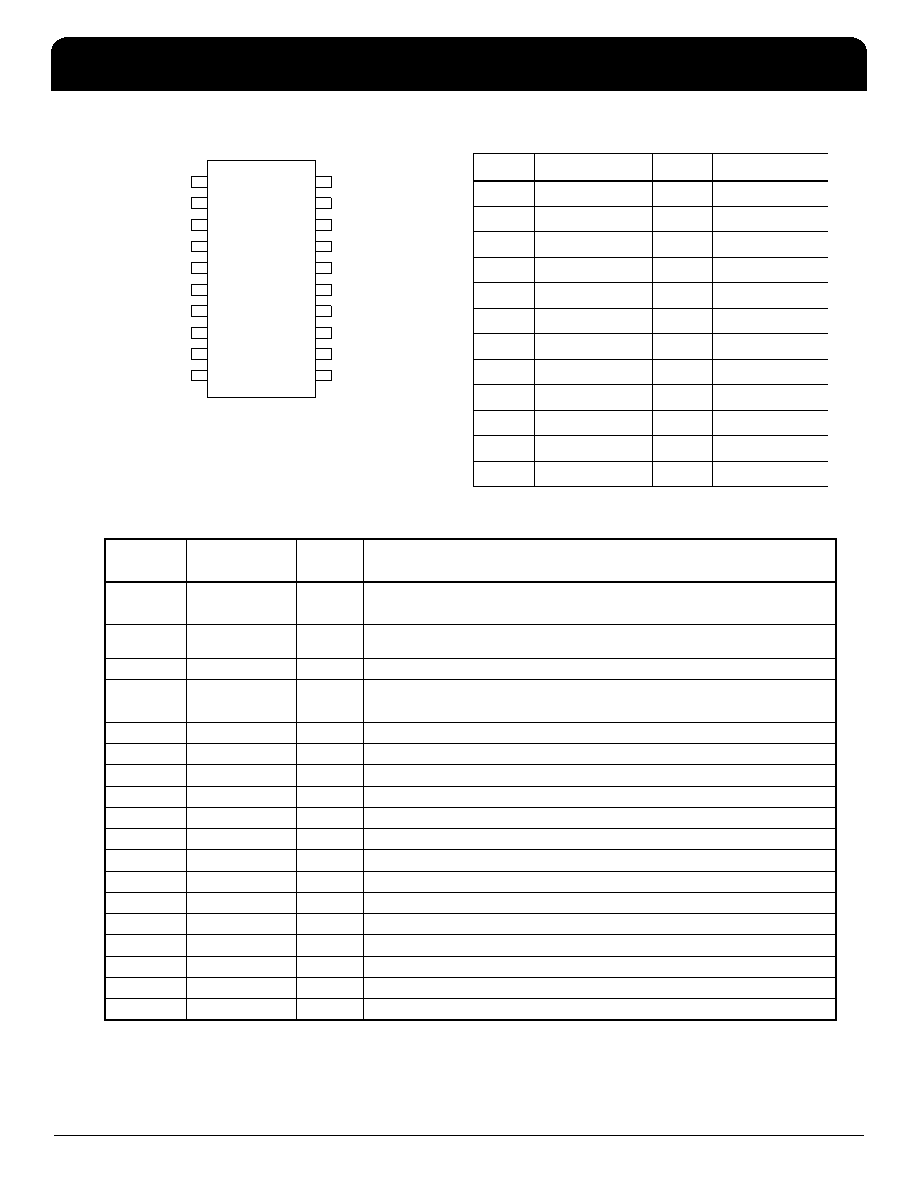
Pin Assignment (ICS552A-01—A mode)
Multiplier Select Table
Pin Descriptions (ICS552A-01—A mode)
16
1
15
2
14
DC
S0
3
13
X2
4
12
X1/ICLK
DC
5
11
S2
6
7
VDD
8
GND
S3
VDD
GND
CLK1
CLK5
CLK2
CLK6
9
10
CLK3
CLK7
CLK4
CLK8
20
19
18
17
20-pin (150 mil) SSOP (QSOP)
S1
S3
S2
S1
S0
Multiplier
0
Power Down
00
0
1
x1
00
1
0
x1.333
00
1
x2
01
0
x2.666
01
0
1
x3
01
1
0
x3.333
01
1
x4
10
0
x5
1
0
1
x4.66
10
1
0
x6
1
0
1
Tri-state all
Pin
Number
Pin
Name
Pin
Type
Pin Description
1
DC
—
Do not connect.
2
X2
XO
Crystal connection. Connect to a 10 - 27 MHz fundamental mode crystal.
3X1/ICLK
XI
Crystal connection. Connect to a 10 - 27 MHz fundamental mode crystal or
clock.
4
VDD
Power
Connect to +3.3 V or 5 V. Decouple with pin 6. Must be same as other VDDs.
5
S2
Input
Multiplier Select pin 2 per table above.
6
GND
Power
Connect to ground.
7
CLK1
Output
Output clock 1.
8
CLK2
Output
Output clock 2.
9
CLK3
Output
Output clock 3.
10
CLK4
Output
Output clock 4.
11
S1
Input
Multiplier Select pin 1 per table above
12
CLK5
Output
Output clock 5.
13
CLK6
Output
Output clock 6.
14
GND
Power
Connect to ground.
15
S3
Input
Multiplier Select pin 3 per table above
16
VDD
Power
Connect to +3.3 V or 5 V. Decouple with pin 14. Must be same as other VDDs.
17
CLK7
Output
Output clock 7.
18
CLK8
Output
Output clock 8.
19
DC
—
Do not connect.
20
S0
Input
Multiplier Select pin 0 per table above
发布紧急采购,3分钟左右您将得到回复。
相关PDF资料
ICS557G-05ALF
IC CLK SOURCE QUAD PCI 20-TSSOP
ICS570BT
IC MULTIPLIER/ZDB 8-SOIC
ICS570GI-01T
IC MULTIPLIER/ZDB 8-MSOP
ICS571MLFT
IC BUFFER ZD LOW PH/NOISE 8-SOIC
ICS601G-01LF
IC CLK MULTIPLIER 16-TSSOP
ICS601M-02ILFT
IC CLOCK MULTIPLIER 16-SOIC
ICS601R-25ILF
IC CLOCK MULTIPLIER 1:5 20-SSOP
ICS613MLF
IC CLOCK MULT LOW PHASE 16-SOIC
相关代理商/技术参数
ICS552G-02
制造商:ICS 制造商全称:ICS 功能描述:LOW SKEW 2 INPUT MUX AND 1 TO 8 CLOCK BUFFER
ICS552G02I
制造商:ICS 功能描述:
ICS552G-02I
功能描述:IC CLOCK BUFFER MUX 2:8 16-TSSOP RoHS:否 类别:集成电路 (IC) >> 时钟/计时 - 时钟缓冲器,驱动器 系列:ClockBlocks™ 标准包装:1 系列:HiPerClockS™ 类型:扇出缓冲器(分配),多路复用器 电路数:1 比率 - 输入:输出:2:18 差分 - 输入:输出:是/无 输入:CML,LVCMOS,LVPECL,LVTTL,SSTL 输出:LVCMOS,LVTTL 频率 - 最大:250MHz 电源电压:2.375 V ~ 3.465 V 工作温度:0°C ~ 70°C 安装类型:表面贴装 封装/外壳:32-LQFP 供应商设备封装:32-TQFP(7x7) 包装:- 其它名称:800-1923-6
ICS552G-02ILN
功能描述:IC CLOCK BUFFER MUX 2:8 16-TSSOP RoHS:是 类别:集成电路 (IC) >> 时钟/计时 - 时钟缓冲器,驱动器 系列:ClockBlocks™ 产品培训模块:High Bandwidth Product Overview 标准包装:1,000 系列:Precision Edge® 类型:扇出缓冲器(分配) 电路数:1 比率 - 输入:输出:1:4 差分 - 输入:输出:是/是 输入:CML,LVDS,LVPECL 输出:CML 频率 - 最大:2.5GHz 电源电压:2.375 V ~ 2.625 V 工作温度:-40°C ~ 85°C 安装类型:表面贴装 封装/外壳:16-VFQFN 裸露焊盘,16-MLF? 供应商设备封装:16-MLF?(3x3) 包装:带卷 (TR)
ICS552G-02ILNT
功能描述:IC CLOCK BUFFER MUX 2:8 16-TSSOP RoHS:是 类别:集成电路 (IC) >> 时钟/计时 - 时钟缓冲器,驱动器 系列:ClockBlocks™ 产品培训模块:High Bandwidth Product Overview 标准包装:1,000 系列:Precision Edge® 类型:扇出缓冲器(分配) 电路数:1 比率 - 输入:输出:1:4 差分 - 输入:输出:是/是 输入:CML,LVDS,LVPECL 输出:CML 频率 - 最大:2.5GHz 电源电压:2.375 V ~ 2.625 V 工作温度:-40°C ~ 85°C 安装类型:表面贴装 封装/外壳:16-VFQFN 裸露焊盘,16-MLF? 供应商设备封装:16-MLF?(3x3) 包装:带卷 (TR)
ICS552G-02IT
功能描述:IC CLOCK BUFFER MUX 2:8 16-TSSOP RoHS:否 类别:集成电路 (IC) >> 时钟/计时 - 时钟缓冲器,驱动器 系列:ClockBlocks™ 标准包装:1 系列:HiPerClockS™ 类型:扇出缓冲器(分配),多路复用器 电路数:1 比率 - 输入:输出:2:18 差分 - 输入:输出:是/无 输入:CML,LVCMOS,LVPECL,LVTTL,SSTL 输出:LVCMOS,LVTTL 频率 - 最大:250MHz 电源电压:2.375 V ~ 3.465 V 工作温度:0°C ~ 70°C 安装类型:表面贴装 封装/外壳:32-LQFP 供应商设备封装:32-TQFP(7x7) 包装:- 其它名称:800-1923-6
ICS552G-02T
制造商:ICS 制造商全称:ICS 功能描述:LOW SKEW 2 INPUT MUX AND 1 TO 8 CLOCK BUFFER
ICS552G-03
制造商:ICS 制造商全称:ICS 功能描述:LOW SKEW 1 TO 8 CLOCK BUFFER (4 AT 1X, 4 AT 1/2X)